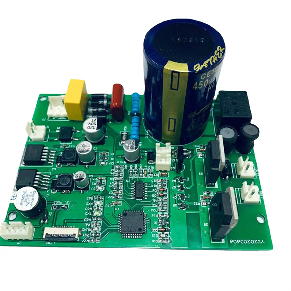
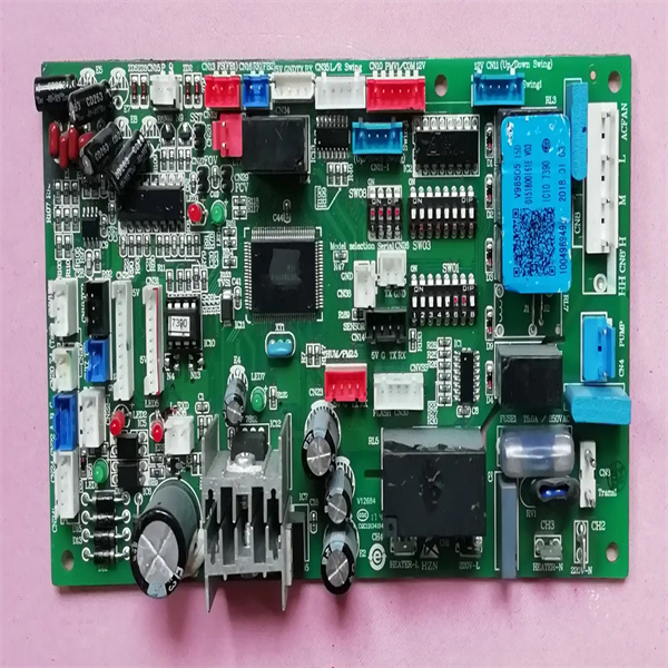
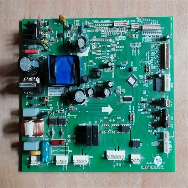
EN Home > showlist
PCB design plays a part in keeping electrical equipment in operation. PCB is an abbreviation of printed circuit board. You can think of a PCB as a puzzle, with pieces that help a device function correctly. You can never work electronics the right way without a good Pdmpump pcb design.
A PCB is composed of various layers that enable the electricity to move around seamlessly. The top layer is the layer of the device where the parts are placed and connected. The middle layers function like highways for the electricity to travel between the parts. The bottom layer provides strength and support. All of these layers collaborate to ensure that the device functions as intended.
When engineers design a PCB, they do it with layouts and schematics, looking ahead at everything. A layout is essentially a map of where everything goes on the Pdmpump pcb design pcbB. It has information about the size, shape and position of each piece.
For an engineer to design a PCB that works as expected and does not cost too much, he must optimize that design., they are performance-cost optimal. They may alter the configuration or select different sections to achieve this balance.

Making the board smaller is one method to maximize the PCB. A smaller Pdmpump printed circuit board pcb design requires less material, which can reduce costs. Engineers can also learn better routes for electricity to follow across the board to boost performance without adding cost.

Understanding the Role of PCB Design in Electronics a Manufacturing important factor in electronic device manufacturing. After the design is complete, it becomes a real thing at a manufacturer. Special machines print the design on a board and add all the parts. This requires careful work to ensure that the end product works well.

Engineers collaborate closely with manufacturers to ensure it gets made right. If issues arise during manufacturing, they may have to tweak things. Engineers and manufacturers will have to work together to build awesome devices people want.