- Home
- About Us
- PDM Pump Products
- Water Pump
- API 610 Series Petrochemic Pump
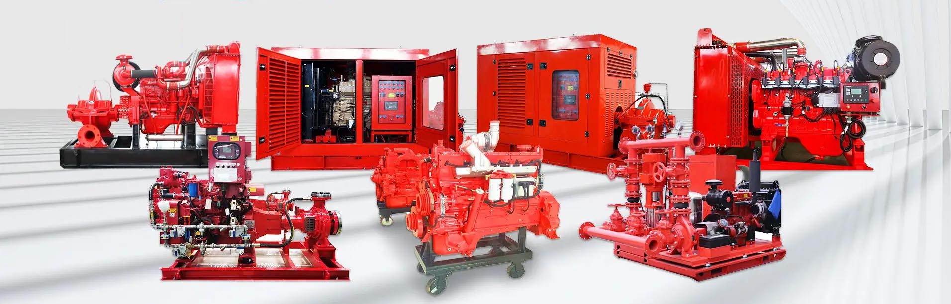
- Fire Fighting Pump NFPA20
- Diesel Engine Pump Set
- Explosion Proof Engine
- Spare Parts & Accesories
- Customized Grinding and Polishing Tool
- II Generation Extended Shaft Electric Straight Die Ginder 2700rpm
- III Generation Extended Shaft Electric Straight die Grinder 27000rpm
- 710W Extended Shaft Electric Straight DieGrinder 33000rpm
- 1500W Extended Shaft Electric StraightDie Grinder 1000--7000rpm Adjustable
- Fillet Weld Angle Grinder
- Belt Electric & Pneumatic Belt Grinder
- Tube Belt Polisher
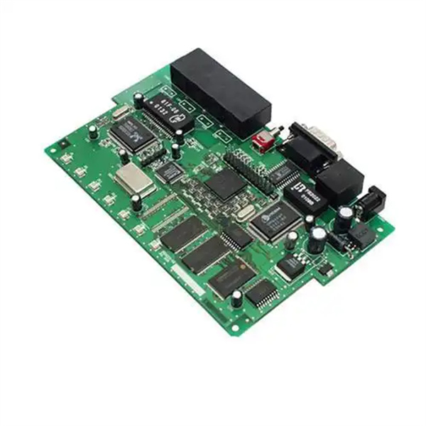
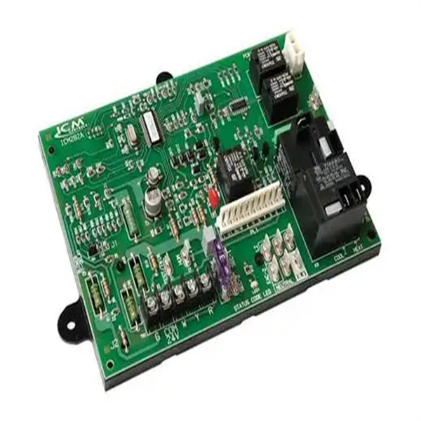
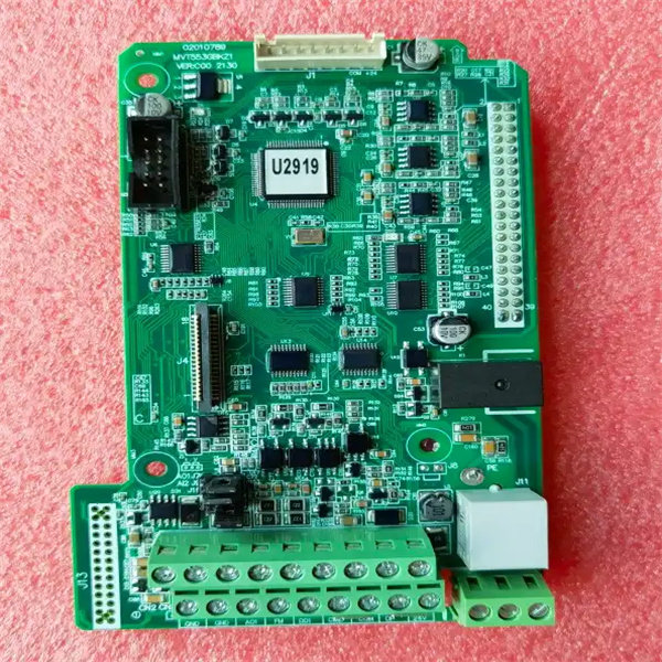
- PDM Electronic Products
- Solutions
- News & Videos
- Contact Us
 EN
EN  EN
EN